AOI Wafer Inspection Tools
Automated Optical Inspection Solutions
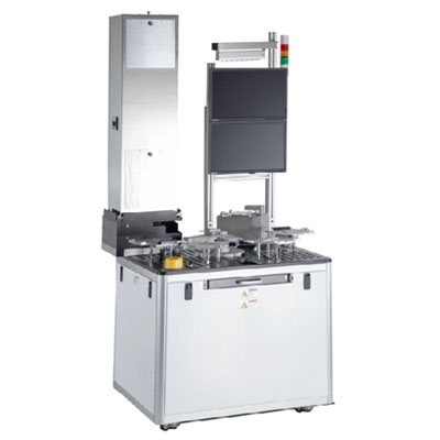
200mm AOI Wafer Inspection
with Makyoh Optics

Side & Backside Mounted
AOI Wafer Inspection Modules

4 Stage Macro
Wafer Inspection System
NADAtech's AOI Wafer Inspection Systems identify wafers with defects and keep them from moving forward in your production line. The AOI module was created to single out wafers with common visible macro defects as well as polishing and postbond wafer surface defects such as dimple and mound defects that are NOT visible to the naked eye, without the use of golden images, while adding minimal time to the inspection process. Our FLEX system allows you to mix and match inspection modules specific for your application to extend the functionality of your system.
- INLINE inspection for wafer sorters
- 150mm / 200mm / 300mm dual brightfield / darkfield wafer inspection
- Brightfield can resolve visible macro defects down to 200um
- Darkfield excels at anything residing above the wafer surface such as particles and scratches
- 150mm / 200mm makyoh optics for surface defect issues
- 1x inspection for both macro and dust defects
- Provides visual inspection for patterned and non patterned wafers on front, back or both sides of wafers
- Completely integrated operation with standard ASCII and SECS / GEM reporting shows defect size and location
- Broad spectrum OMNI color LED lighting + grazing dark field LED
- Dome reflector used for omni-directional illumination
- 15mpixel color CMOS imaging camera and coaxial light port
- Excellent for 3D type defects such as EPI “volcanoes”
- Image stack post processing shows “repeaters” and defect clustering
Additional Wafer Inspection Modules
Further Customize Your Wafer Sorter System

Bright Light Inspection

Edge Inspection

Surface Inspection
Extend the functionality of your system with NADAtech’s Sorter+ Inspection Solutions. Find defects on wafer surfaces and edges using a variety of specially designed applications without adding extra equipment to your production floor.
Bright Light Inspection
+Gyro

- Front and backside bright light inspection
- Optional full rotation
- 150mm / 200mm / 300mm
- Wafer top-side and bottom-side visual inspection
- Joystick control or programmable recipe control with pass/fail button
- Function can be added to any typical sorting recipe
Bright Light Inspection
+EdgeGyro

- Edge handling only
- Typical bright light inspection for substrate manufacturers
- Front and backside bright light inspection
- Full infinite rotation
- 150mm / 200mm / 300mm
- Wafer top-side and bottom-side visual inspection
- Joystick control or programmable recipe control with pass/fail button
- Function can be added to any typical sorting recipe
Bright Light Inspection
+Gimbal

- Front side only bright light inspection
- Full gimbaling action for topside visual inspection
- Joystick control or programmable recipe control with pass/fail button
- Function can be added to any typical sorting recipe
Scribe Location Inspection
+SLI

- Option for any system using OCR
- Measures scribe location against a qualified location
- Automated characterization
- Automated inspection
- Function can be added to any typical sorting recipe
- Includes SECS / GEM reporting for X / Y and linear offests
- Limits monitoring and alarms
Wafer Edge Inspection
+ChipChecker

- Top and bottom bevel inspection option
- Function can be added to any typical sort recipe
- Scans wafer bevel for cracks and chips after Align / OCR function
- Standard ASCII and SECS / GEM reporting with defect size and location
- Optional image capture and industry standard XY Report Formating
- Captures defects down to 0.5mm, with latest generation seeing defects down to 60um
- Version 1.0 flags failed wafers and shows number of chips >0.3mm defect bare wafer / >0.5mm defect processed
- Version 2.0 easily detects bonding edge problems and captures multi-tiff images of each chip for K L A R F, recording chip location and size
Wafer Surface Inspection
+Dimple

- Surface defects are detected and measured using fully integrated Hologenix optics
- Uses defocused optics for finding surface defects ( dimples or mounds )
- Typical for wafer polishing defects
- Perfect for finding Post CMP over and under polished areas
- Also used for Post wafer bond MEMS defect inspection
- 150mm / 200mm / 300mm versions
- Whole wafer image processing or magnified version are available
- Optional stocker and agv integrated e84 delivery